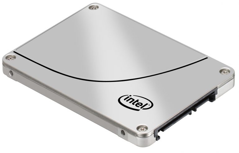
Intel has announced it will use 32-layer 3D NAND flash chips from now on. While this might not seem like important news, in reality it is as it will have long-term consequences for the chip maker as well as consumers. One good outcome is that this technology will allow Intel to build solid-state drives that will be larger than 10 TB. Suddenly 32-layer 3D NAND becomes a big thing, doesn’t it?
The magic behind 3D NAND is that the technology uses three-dimensional NAND die stacking, where chip layers are oriented vertically as opposed to horizontal planar structures. This allows for higher capacities and better power efficiency – all being key requirements for better and larger SSDs. Until now Samsung has been the only company to use the technology in its own products.
Intel will reportedly use 256-gigabit MLC NAND flash chips that will consist of 32 layers and they will be available in 384-gigabit TLC configurations too. The new Intel chips will likely use a larger process node that will be around 40 nm. This is due to the fact that flash memory reliability goes down as process nodes shrink hence by using 40 nm technology Intel 3D NAND-based SSDs will be more reliable. If Intel stacks hundreds of layers of NAND per die then SSDs will hit 10 TB capacities, something which is true for Samsung as well.
Intel plans to release its first 32-layer 3D NAND SSDs in 2015 but they will likely target the enterprise segment at first and then when prices go down they will reach consumers. This also holds true for the projected 10+ TB solid-state drives in the near future.
Source: Extremetech.com

