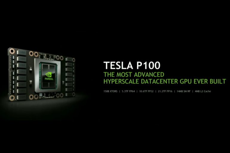
The US GPU maker NVIDIA has unveiled the first product based on the company’s Pascal GPU architecture – the Tesla P100 HPC board. The device is designed for use with ultra-high density supercomputing cluster boxes so unfortunately you will not be able to put a Pascal GPU in your computer just yet but they are on their way to us. Anyway the Tesla P100 is a tech wonder in its own way so it definitely deserves a word.
The new NVIDIA HPC board houses a Pascal GPU that contains the amazing 15 billion transistors. The GPU also features a 4096-bit HBM2 memory interface that is wired to four 3D HBM2 stacks just like in AMD’s Fiji GPU. All this hardware is put on a fiberglass substrate that is rooted into the board PCB over a ball-grid array. The GPU, the wafer and the memory put together house an incredible number of transistors – 150 billion! This is all possible due to the usage of a 16 nm FinFET production process but even then the GPU occupies 600 mm² of area.
As you can see from the tech specs the Tesla P100 packs quite a bit of punch – the card offers a double-precision (FP64) compute performance of 5.3 TFLOPs, single precision (FP32) performance of 10.6 TFLOPs and FP16 performance of 21.2 TFLOPs. In addition to this the chip has registers as big as 14.2 MB and 4 MB of L2 cache as well as NVLink technology by NVIDIA, which provides 80 GB/sec of memory bandwidth per direction and 160 GB/sec in both directions.
The new NVIDIA Tesla P100 HPC board is now in volume production. Market availability is expected a bit later.
Source: NVIDIA
