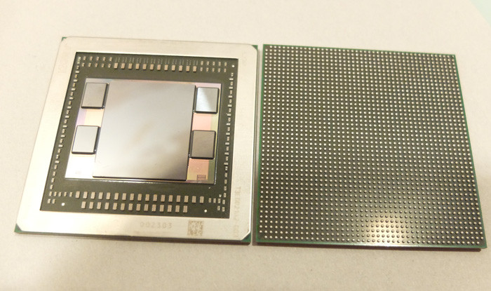
A week after the launch of the new Radeon R9 300-series and the announcement of the Radeon R9 Fury X we have gotten the block diagram of the new revolutionary chip.
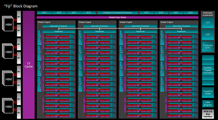
As you can see Fiji comes with four Shader Engine clusters, just like the older Hawaii GPU, but this time Fiji sports 16 CGN Compute Units, up from the 11 per cluster featured in Hawaii. In addition Fiji likely uses a new revision of the Graphics Core Next architecture. The rest is well known but very impressive – you can see the new HBM memory directly connected to the chips and you can see that Fiji has 4096 stream processors, 256 TMUs (up from 176 in Hawaii) and 64 ROPs. The HBM memory pumps data through an insanely wide 4096-bit bus and that’s why the memory works at just 500 MHz. Thanks to the very wide memory bus the low clock speed of the memory is not a problem – in fact Fiji boasts one of the highest memory bandwidth results – 512 GB/sec, which is impressive to say the least.
Speaking of the HBM memory, unfortunately it won’t be overclockable so you are stuck to 500 MHz of clock speed. The good news is that the Fiji GPU can be made to run faster from its 1050 MHz to 1150 MHz relatively easy or so various online sources claim.
Source: Legit Reviews